


Wafer Positioning and Alignment
Release Date:2025-05-14 Source: View count256
In the semiconductor manufacturing process, precise wafer positioning and alignment are critical. Piezoelectric technology enables accurate positioning and alignment of wafers during processing by using piezoelectric ceramics as actuators. By applying appropriate piezoelectric signals, the piezoelectric actuator can quickly and precisely control the position and orientation of the wafer, ensuring the accuracy and consistency of each process step. Piezoelectric technology is used for wafer positioning and alignment during wafer fabrication and handling. Its advantages include high precision, fast response speed, and excellent stability, meeting the stringent requirements of semiconductor processes for positioning and alignment.

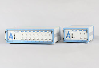
Figure 1 - Wafer Positioning Stage Figure 2 - High-Precision Wafer Positioning System

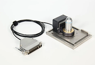
Figure 3 - Wafer positioning stage with nanometer-level accuracy
In the semiconductor manufacturing process, precise wafer positioning and alignment are critical. Piezoelectric technology enables accurate positioning and alignment of wafers during processing by using piezoelectric ceramics as actuators. By applying appropriate piezoelectric signals, the piezoelectric actuator can quickly and precisely control the position and orientation of the wafer, ensuring the accuracy and consistency of each process step. Piezoelectric technology is used for wafer positioning and alignment during wafer fabrication and handling. Its advantages include high precision, fast response speed, and excellent stability, meeting the stringent requirements of semiconductor processes for positioning and alignment.
Figure 1 - Wafer Positioning Stage Figure 2 - High-Precision Wafer Positioning System
Figure 3 - Wafer positioning stage with nanometer-level accuracy
- Prev:none
- Next:Photolithography