


Photolithography
Release Date:2025-05-14 Source: View count160
Breakthroughs in global digitalization are inseparable from the latest generation of integrated circuits manufactured by lithography technology. Both the processing of wafers in lithography and the metrology of components such as masks require ultra-precise positioning technology. Typically, systems operate in harsh environments with vacuum and high-energy radiation, allowing only a limited selection of materials. Positioning systems based on piezoelectric drive technology combine a highly compact footprint with extreme precision to meet the special requirements of lithography applications.

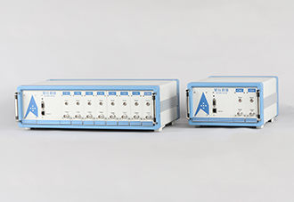
Figure 1 - Schematic Diagram of a Lithography System Based on Piezoelectric Actuators

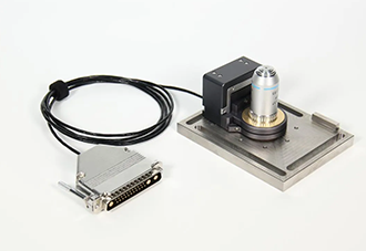
Figure 2 - Multi-DOF Piezo Stage Used in Lithography Equipment
Breakthroughs in global digitalization are inseparable from the latest generation of integrated circuits manufactured by lithography technology. Both the processing of wafers in lithography and the metrology of components such as masks require ultra-precise positioning technology. Typically, systems operate in harsh environments with vacuum and high-energy radiation, allowing only a limited selection of materials. Positioning systems based on piezoelectric drive technology combine a highly compact footprint with extreme precision to meet the special requirements of lithography applications.
Figure 1 - Schematic Diagram of a Lithography System Based on Piezoelectric Actuators
Figure 2 - Multi-DOF Piezo Stage Used in Lithography Equipment